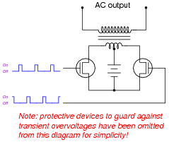
DC-AC电源转换器电路的常见拓扑使用一对晶体管to switch DC current through the center-tapped winding of a step-up transformer, like this:
|
|
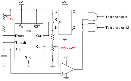
为了使这种电路正常运行,晶体管“启动”信号必须精确地同步,以确保两者永远不会同时打开。以下示意图显示了一个电路以生成必要的信号:

|
|
Explain how this circuit works, and identify the locations of the frequency control and pulse duty-cycle control potentiometers.
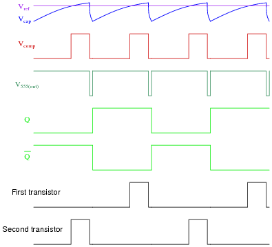
定时图值得一千个单词:
|
|
|
|
后续问题:您必须移动哪个方向,以增加该电路的输出频率?您还必须将占空比电位计的哪个方向也增加?
挑战问题:假设您在没有示波器的利益的情况下对该电路进行了原型。您如何测试电路以确保最终的输出脉冲到晶体管永远不会同时处于“高”逻辑状态?假设您的零件分类配有发光二极管和其他被动组件。
This question is an exercise in schematic diagram and timing diagram interpretation. By the way, I have built and tested this circuit and I can say it works very well.
示意图中显示的齐纳二极管在那里吸收瞬态电压,当MOSFET关掉。解释这些瞬态起源于哪里,以及如果zener diodes不在那里。
Energy stored in the电感当MOSFET关闭并且磁场崩溃时,初级绕组必须移至某个地方。齐纳二极管提供了一种安全的方法来消除这种存储的能量。
后续问题:当逆变器电路卸载(没有连接到变压器的次级的交流负载)时,齐纳二极管可能会变暖。有趣的是,当连接交流负载时,这些相同的二极管将冷却。解释为什么这是。
Energy storage and transfer are vitally important concepts to grasp for power conversion circuits such as this. The follow-up question was the result of actually testing this inverter circuit and monitoring its performance loaded and unloaded.
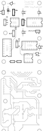
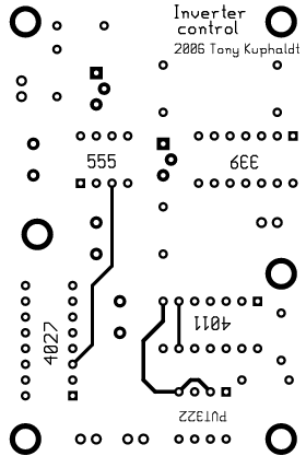
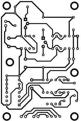
Examine these check plot images from a PCB drafting program, for a control board based on this inverter circuit design. Both the top and bottom copper layer plots are shown from the perspective of the board’s top side. The six large “pads” around the periphery of the board are actually holes for mounting screws:
|
|
|
|
|
|
|
|
|
标记离散组件(电阻,电容器和二极管)进入PCB的位置,并确定板布局上哪些集成电路在示意图中执行哪些功能。注意:每个IC上的方垫标记数字1。
我会让你做这项工作。说cuss your answers with your classmates!
This is an exercise in datasheet research and layout tracing. One potentially confusing aspect of the PCB shown is that I have a diode placed in the circuit for “idiot-proofing” in the event of reverse power supply connections.
如果您想知道,即使没有显示丝网印刷,IC零件编号也出现在“顶铜”检查图上的原因是因为我实际上将零件编号写为铜层的一部分。这纯粹是出于经济目的而进行的:我的PCB供应商提供的“裸骨头”协议没有丝网印刷功能,我仍然想在板上有IC标签。


